
Fast switching 800V N-Channel Power MOSFET
- Product Description
-
800V N-Channel Power MOSFET
YZPST-SP50N80FX
FEATURES
Fast switching
100% avalanche tested
Improved dv/dt capability
APPLICATIONS
Switch Mode Power Supply (SMPS)
Uninterruptible Power Supply (UPS)
Power Factor Correction (PFC)
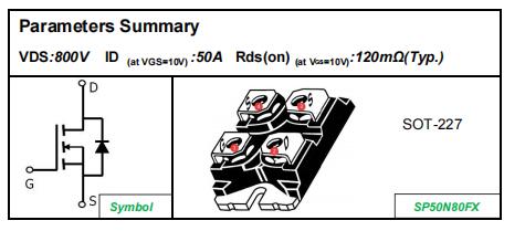
Device Ordering Marking Packing Information
Ordering Number
Package
Marking
Packing
SP50N80FX
SOT-227
SP50N80FX
Tube
Absolute Maximum Ratings TC = 25ºC, unless otherwise noted
Parameter
Symbol
Value
Unit
Drain-Source Voltage (VGS = 0V)
VDSS
800
V
Continuous Drain Current
ID
50
A
Pulsed Drain Current (note1)
IDM
200
A
Gate-Source Voltage
VGSS
±30
V
Single Pulse Avalanche Energy (note2)
EAS
4500
mJ
Repetitive Avalanche Energy (note1)
EAR
60
mJ
Power Dissipation (TC = 25ºC)
PD
690
W
Operating Junction and Storage Temperature Range
TJ, Tstg
-55~+150
ºC
Caution: Stresses greater than those listed in the “Absolute Maximum Ratings” may cause permanent damage to the device.
Thermal Resistance
Parameter
Symbol
Value
Unit
Thermal Resistance, Junction-to-Case
RthJC
0.18
ºC/W
Thermal Resistance, Junction-to-Ambient
RthJA
40
Specifications TJ = 25ºC, unless otherwise noted
Parameter
Symbol
Test Conditions
Value
Unit
Min.
Typ.
Max.
Static
Drain-Source Breakdown Voltage
V(BR)DSS
VGS = 0V, ID = 250µA
800
--
--
V
Zero Gate Voltage Drain Current
IDSS
VDS =800, VGS = 0V, TJ = 25ºC
--
--
1.0
μA
Gate-Source Leakage
IGSS
VGS = ±30V
--
--
±100
nA
Gate-Source Threshold Voltage
VGS(th)
IDS = 250µA
2.5
--
4.5
V
Drain-Source On-Resistance (Note3)
RDS(on)
VGS = 10V, ID = 25A
--
120
130
mΩ
Dynamic
Input Capacitance
Ciss
VGS = 0V, VDS = 25V, f = 1.0MHz
--
14600
--
pF
Output Capacitance
Coss
--
1300
--
Reverse Transfer Capacitance
Crss
--
66
--
Total Gate Charge
Qg
VDD =400V, ID =50A, VGS = 10V
--
360
--
nC
Gate-Source Charge
Qgs
--
80
--
Gate-Drain Charge
Qgd
--
120
--
Turn-on Delay Time
td(on)
VDD = 400V, ID =50A, RG = 10 Ω
--
110
--
ns
Turn-on Rise Time
tr
--
200
--
Turn-off Delay Time
td(off)
--
160
--
Turn-off Fall Time
tf
--
185
--
Drain-Source Body Diode Characteristics
Continuous Body Diode Current
IS
TC = 25 ºC
--
--
50
A
Pulsed Diode Forward Current
ISM
--
--
400
Body Diode Voltage
VSD
TJ = 25ºC, ISD = 25A, VGS = 0V
--
--
1.4
V
Reverse Recovery Time
trr
VGS = 0V,IS = 50A,
diF/dt =100A /μs
--
520
--
ns
Reverse Recovery Charge
Qrr
--
5.0
--
μC
Notes
1. Repetitive Rating: Pulse width limited by maximum junction temperature
2. VDD = 50V, RG = 25 Ω, Starting TJ = 25 ºC
Pulse Test: Pulse width ≤ 300μs, Duty Cycle ≤ 1%


Product Inquiry
We will contact you within one working day. Please pay attention to your email.
* Note: Please be sure to fill in the information accurately and keep the communication unblocked. We will get in touch with you as soon as possible.

Do you want to know more product details? Send us a consultation!
We will contact you within one working day. Please pay attention to your email.
CONTACT
Tel:+86-514-87360558、87782298、87782296
Fax:+86-514-87782297、87367519
E-mail: info@stt.tm / yzpst@pst888.com
WhatsApp: +8613805278321
SKYPE:Microsoft Teams ID:326880628@qq.com
Link: www.yzpst.com / www.pst888.com / www.yzpst.net


