
C712L thyristor power controller KT55CT
- Product Description
-
HIGH POWER THYRISTOR FOR INVERTER AND CHOPPER APPLICATIONS
YZPST-C712L
Features:
. All Diffused Structure
. Center Amplifying Gate Configuration
. Blocking capabilty up to 2100 volts
. Guaranteed Maximum Turn-Off Time
. High dV/dt Capability
. Pressure Assembled Device
ELECTRICAL CHARACTERISTICS AND RATINGS
Blocking - Off State
VRRM (1)
VDRM (1)
VRSM (1)
2000
2000
2100
VRRM = Repetitive peak reverse voltage
VDRM = Repetitive peak off state voltage
VRSM = Non repetitive peak reverse voltage (2)
Repetitive peak reverse leakage and off state leakage
IRRM / IDRM
20 mA
90 mA (3)
Critical rate of voltage rise
dV/dt (4)
800 V/msec
Conducting - on state
Parameter
Symbol
Min.
Max.
Typ.
Units
Conditions
Average value of on-state current
IT(AV)
1185
A
Sinewave,180o conduction,Tc=80oC
RMS value of on-state current
ITRMS
1700
A
Nominal value
Peak one cPSTCle surge
(non repetitive) current
ITSM
-
18500
A
A
8.3 msec (60Hz), sinusoidal wave-
shape, 180o conduction, Tj = 125 oC
10.0 msec (50Hz), sinusoidal wave-
shape, 180o conduction, Tj = 125 oC
I square t
I2t
1.66x10⁶
A2s
8.3 msec and 10.0 msec
Latching current
IL
-
mA
VD = 24 V; RL= 12 ohms
Holding current
IH
-
mA
VD = 24 V; I = 2.5 A
Peak on-state voltage
VTM
1.45
V
ITM = 1000 A; Duty Cycle £ 0.01%; Tj =1 25 oC
Critical rate of rise of on-state
current (5, 6)
di/dt
800
A/ms
Switching from VDRM £ 1000 V,
non-repetitive
Critical rate of rise of on-state
current (6)
di/dt
200
A/ms
Switching from VDRM £ 1000 V
Gating
Parameter
Symbol
Min.
Max.
Typ.
Units
Conditions
Peak gate power dissipation
PGM
100
W
tp = 40 us
Average gate power dissipation
PG(AV)
5
W
Peak gate current
IGM
-
A
Gate current required to trigger all units
IGT
-
120
-
mA
mA
mA
VD = 6 V;RL = 3 ohms;Tj = -40 oC
VD = 6 V;RL = 3 ohms;Tj = +25 oC
VD = 6 V;RL = 3 ohms;Tj = +125oC
Gate voltage required to trigger all units
VGT
-
3.0
-
V
V
V
VD = 6 V;RL = 3 ohms;Tj = -40 oC
VD = 6 V;RL = 3 ohms;Tj = 0-125oC
VD = Rated VDRM; RL = 1000 ohms;
Tj = + 125 oC
Peak negative voltage
VGRM
20
V
Dynamic
Parameter
Symbol
Min.
Max.
Typ.
Units
Conditions
Delay time
td
-
0.7
ms
ITM = 50 A; VD = Rated VDRM
Gate pulse: VG = 20 V; RG = 20 ohms; tr = 0.1 ms; tp = 20 ms
Turn-off time (with VR = -50 V)
tq
40
-
ms
ITM = 1000 A; di/dt = 25 A/ms;
VR ³ -50 V; Re-applied dV/dt = 20 V/ms linear to 80% VDRM; VG = 0;
Tj = 125 oC; Duty cPSTCle ³ 0.01%
Reverse recovery charge
Qrr
*
mC
ITM = 1000 A; di/dt = 25 A/ms;
VR ³ -50 V
HERMAL AND MECHANICAL CHARACTERISTICS AND RATINGS
Parameter
Symbol
Min.
Max.
Typ.
Units
Conditions
Operating temperature
Tj
-40
+125
oC
Storage temperature
Tstg
-40
+125
oC
Thermal resistance - junction to case
RQ (j-c)
0.023
-
oC/W
Double sided cooled
Single sided cooled
Thermal resistamce - case to sink
RQ (c-s)
0.0075
-
oC/W
Double sided cooled *
Single sided cooled *
Mounting force
P
22.2
26.6
kN
Weight
W
-
g
About
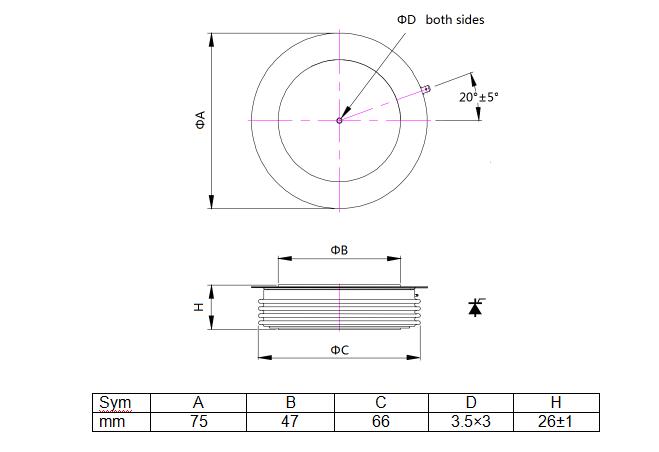
CASE OUTLINE AND DIMENSIONS


Product Inquiry
We will contact you within one working day. Please pay attention to your email.
* Note: Please be sure to fill in the information accurately and keep the communication unblocked. We will get in touch with you as soon as possible.

Do you want to know more product details? Send us a consultation!
We will contact you within one working day. Please pay attention to your email.
CONTACT
Tel:+86-514-87360558、87782298、87782296
Fax:+86-514-87782297、87367519
E-mail: info@stt.tm / yzpst@pst888.com
WhatsApp: +8613805278321
SKYPE:Microsoft Teams ID:326880628@qq.com
Link: www.yzpst.com / www.pst888.com / www.yzpst.net


