RGN65C035 Lower BOM cost 650V Super-GaN FET in TO-247
- 产品描述
-
650V Super-GaN FET in TO 247 P/N: YZPST-RGN65C035FeaturesEasy to drive—compatible with standard gate driversLow conduction and switching lossesLow Qrr of 175nC—no free-wheeling diode requiredGSD pin layout improves high speed designJEDEC-qualified GaN technologyRoHS compliant and Halogen-freeBenefitsIncreased efficiency through fast switchingIncreased power densityReduced system size and weightEnables more efficient topologies—easy to implement bridgeless totem-pole designsLower BOM costApplicationsRenewable energyIndustrialAutomotiveTelecom and datacomServo motors
 Absolute Maximum Ratings (TC=25°C unless otherwise stated)
Symbol
Parameter
Limit Value
Unit
ID25°C
Continuous drain current @TC=25 °C a
50
A
ID100°C
Continuous drain current @TC=100 °C a
31.5
A
IDM
Pulsed drain current (pulse width: 10µs)
240
A
VDSS
Drain to source voltage
650
V
VTDS
Transient drain to source voltage b
800
V
VGSS
Gate to source voltage
±18
V
PD25 °C
Maximum power dissipation
178
W
TJ
Operating junction temperature
-55 to +150
°C
TS
Storage temperature
-55 to +150
°C
TCSOLD
Soldering peak temperature c
260
°C
Thermal Resistance
Symbol
Parameter
Typical
Unit
RΘJC
Junction-to-case
0.7
°C/W
RΘJA
Junction-to-ambient
40
°C/W
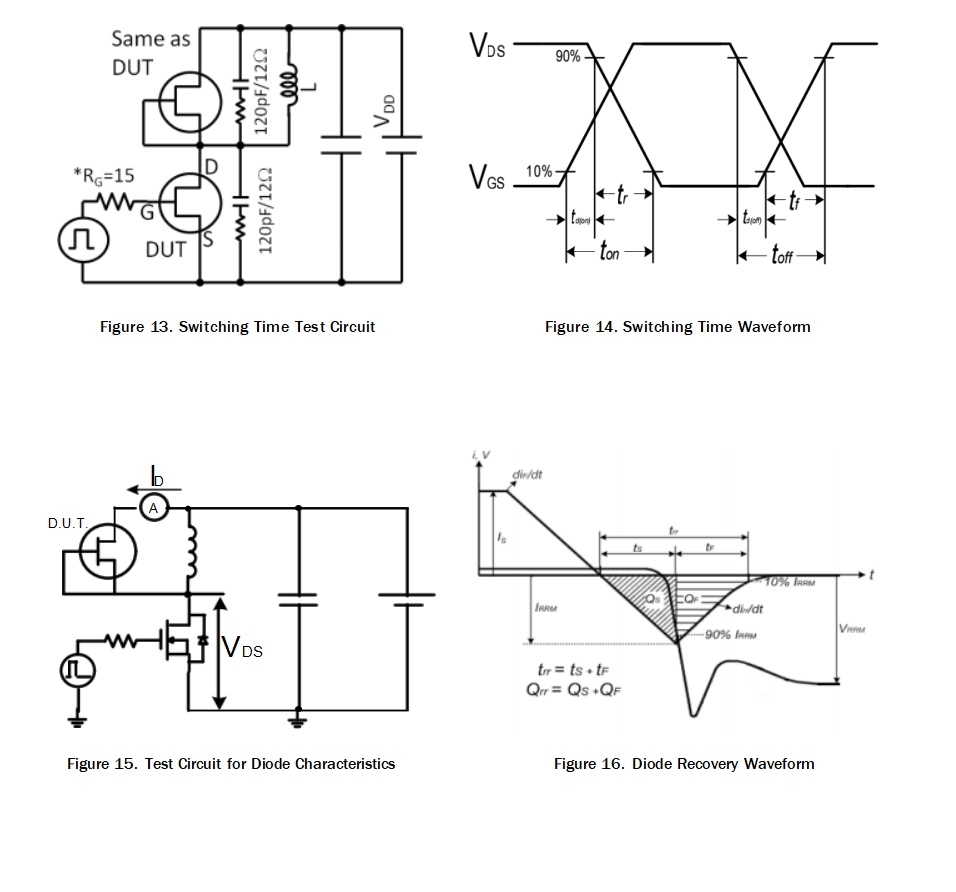
Test Circuits and Waveforms

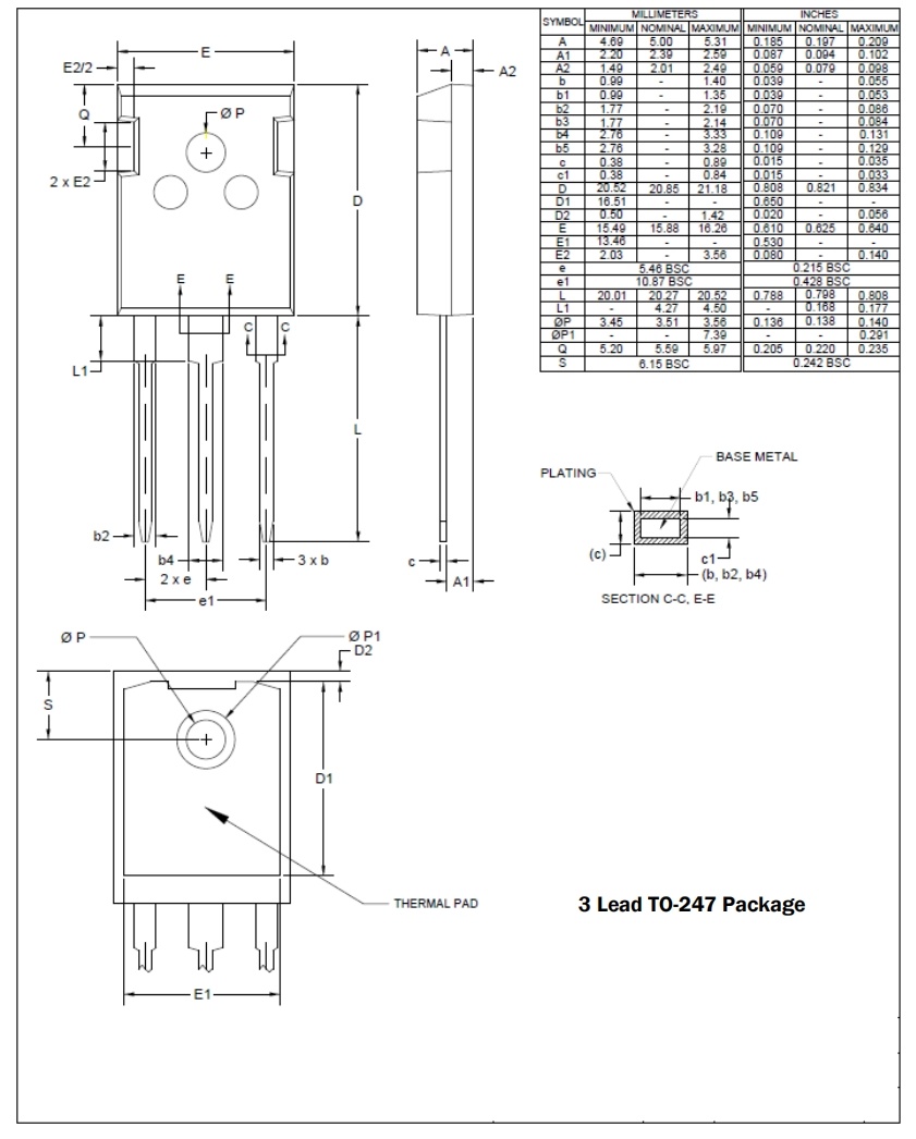
Mechanical

Product Inquiry
We will contact you within one working day. Please pay attention to your email.
* Note: Please be sure to fill in the information accurately and keep the communication unblocked. We will get in touch with you as soon as possible.


